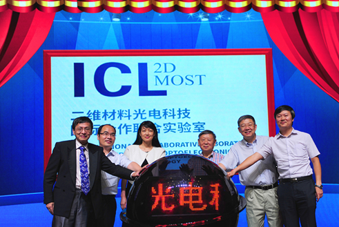
June 2 morning, the two-dimensional materials optoelectronics Science and Technology Department of International Cooperation Laboratory in our University International Conference Hall officially launched.

The establishment of the joint Laboratory of International Cooperation of the two-dimensional materials optoelectronics Science and Technology Ministry of Education is a useful exploration and practice for the Ministry of Education to guide the internationalization of laboratories, which emphasizes the research and development of original innovation technology, and establishes the logo of International Open Laboratory with the concept of openness, inclusiveness, synergyLaboratory director Fan Yuan, academician of Chinese Academy of Engineering, distinguished professor, Doctoral tutor, Chinese director of Optoelectronic Technology Co-Innovation center, the country has outstanding contributions to young experts, the national Outstanding science and technology workers.The laboratory is located in Shenzhen University, is the Ministry of Education in the two-dimensional materials in recent years in the field of development achievements Affirmation, is the Ministry of Education in the deep to create an international laboratory of confidence embodiment.
At present, the two-dimensional materials Optoelectronics Technology Ministry of Education International Cooperation Laboratory in Shenzhen University has a fixed scientific research staff of 19, one of the Chinese Academy of Engineering 1, Singapore Academy of Natural Sciences 2, Asia-Pacific Materials Materials Science and Technology 1, Singapore, the highest scientific honorary President Award Winners 2, the National youth thousands of 3 people, all with a doctorate;Postdoctoral in the station more than 60, more than 20 graduate students.The laboratory has a nd glass high-power laser system, high-power middle-infrared laser production and amplification system, wide-band spectrum measurement and analysis system, microwave photon technology, vortex optical communication system, chemical vapor deposition system (tubular furnace CVD,PECVD), confocal spectral system, Leica Microscope, Semiconductor electrical characterization System, two-particle beam sputtering thin film deposition system, such as large equipment more than 40 sets, more than 1 million large equipment 11 sets, equipment value of more than 49 million yuan.It covers the research needs of material preparation, structure and photoelectric characterization and application, and forms a complete system of scientific research platform and talent training base.Nearly three years, the laboratory has access to scientific research projects and talent programs to support nearly hundred, the total funds nearly billion, basically covering the National Fund committee major Projects, key projects, surface projects, youth projects;National science and technology major special projects, 863, 973 plans and other national issues.More than 20 patent applications, published more than 500 high-level scientific research papers.
Laboratories facing the forefront of international optoelectronic technology, to carry out collaborative innovation, service national strategic needs;Based on the research and development of new materials such as two-dimensional atomic crystals, this paper aims to develop the basic research and application development of the next generation optoelectronic devices and systems.In information electronics, detection sensors, green energy, biomedicine and other directions to achieve a number of major scientific breakthroughs, the output of international advanced/leading first-class results, to achieve transformation and industrialization of results.

